Product Introduction: N-Type Silicon Wafers (Dummy Grade)
Silicon wafers are a cornerstone of the semiconductor industry, serving as the substrate upon which integrated circuits, sensors, and other electronic components are built. Among these, N-type silicon wafers, especially in dummy grade, are extensively used in processes that demand high-quality substrates without the cost of prime-grade materials. These wafers are fabricated in multiple diameters—2-inch, 4-inch, 6-inch, 8-inch, and 12-inch—to cater to diverse industry applications. This introduction provides a comprehensive overview of their properties, specifications, and applications, with a particular focus on dummy-grade N-type silicon wafers.
1. Material and Doping
N-type silicon wafers are derived from single-crystal silicon, a highly pure material produced through advanced crystal growth methods such as the Czochralski (CZ) or Float Zone (FZ) processes. The "N-type" designation refers to the doping with elements such as phosphorus, arsenic, or antimony, which donate extra electrons, making the silicon conductive.
Dummy-grade wafers, in contrast to prime-grade wafers, are designed for non-critical applications. These may include testing, calibration, or training purposes, where the electrical, mechanical, and optical performance does not need to meet the stringent specifications required for active semiconductor devices.
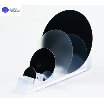
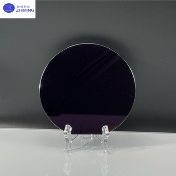
2. Diameter Variants
2-Inch Wafers (50.8 mm):
These are typically used in small-scale laboratories, research institutions, and applications requiring compact processing equipment. Their small size makes them cost-effective for experimental use.
4-Inch Wafers (100 mm):
Widely used in R&D and pilot-scale production lines, 4-inch wafers strike a balance between availability, cost, and compatibility with legacy semiconductor fabrication equipment.
6-Inch Wafers (150 mm):
The 6-inch diameter is common in industrial and specialty electronics production. It is a standard size for MEMS (Micro-Electro-Mechanical Systems) and sensor manufacturing.
8-Inch Wafers (200 mm):
These wafers are prevalent in mainstream semiconductor manufacturing. They offer a larger surface area, enabling higher production volumes per wafer.
12-Inch Wafers (300 mm):
At the cutting edge of the industry, 12-inch wafers provide even greater economies of scale. Despite their high initial cost, they are favored for mass production in high-volume, state-of-the-art fabrication facilities.
3. Key Specifications
| Parameter | Specifications |
|---|
| Material | Single-Crystal Silicon (N-Type) |
| Dopant | Phosphorus, Arsenic, or Antimony |
| Orientation | <100> or <111>, based on application |
| Diameter Options | 2-inch, 4-inch, 6-inch, 8-inch, 12-inch |
| Thickness Range | Customized based on diameter (e.g., 500 µm to 775 µm) |
| Surface Finish | SSP (Single Side Polished) or DSP (Double Side Polished) |
| Resistivity | Ranges from 1–10 Ω·cm, based on customer needs |
| Thermal Stability | High thermal conductivity and low thermal expansion |
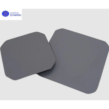
4. Dummy Grade Characteristics
Dummy-grade wafers serve as cost-effective alternatives to prime-grade wafers. While they meet basic requirements for dimensional accuracy, flatness, and surface polish, they are not subjected to the rigorous testing and certification that prime wafers undergo. Some key characteristics include:
- Surface Quality: Single-side polished (SSP) with minor imperfections acceptable for non-critical processes.
- Flatness and Thickness Uniformity: Sufficient for calibration and equipment testing.
- Resistivity Range: Broader tolerance compared to prime-grade wafers, suitable for process optimization.
These attributes make dummy wafers ideal for functions like thermal cycle testing, dry etching, and chemical-mechanical planarization (CMP) equipment evaluations.
5. Applications
Dummy-grade N-type silicon wafers are integral to several stages of semiconductor processing and other industrial practices:
a) Semiconductor Equipment Testing
Dummy wafers are widely used for evaluating and calibrating semiconductor manufacturing equipment, such as lithography systems, etching tools, and deposition machines. This minimizes the risk of damaging costly prime wafers during early-stage tests.
b) CMP and Thin Film Deposition
Chemical Mechanical Planarization (CMP) processes benefit from dummy wafers as substrates for slurry testing and equipment qualification. Similarly, thin-film deposition systems use dummy wafers to fine-tune parameters like thickness uniformity and material adhesion.
c) Research and Development
R&D facilities rely on dummy wafers for prototyping new designs or processes, reducing costs and waste during iterative testing.
d) Training and Education
Universities and training centers use dummy wafers for hands-on instruction in semiconductor manufacturing techniques.
e) Packaging and Handling
Dummy wafers often play a role in logistics, such as testing the performance of wafer carriers, cassettes, and automated handling systems.
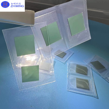
6. Packaging and Clean Room Handling
All dummy-grade wafers are packaged under stringent cleanroom conditions to prevent contamination. Typically, they are enclosed in cassettes of 25 wafers and sealed in Class 100 environments. This ensures that they arrive in optimal condition for immediate use.
7. Advantages of Dummy Grade Wafers
- Cost Efficiency: Significant savings compared to prime wafers, particularly for non-critical processes.
- Versatility: Available in a variety of diameters and thicknesses, catering to diverse industry needs.
- Risk Mitigation: Allows testing and optimization without risking high-value substrates.
- Sustainability: Helps reduce material waste during equipment trials and R&D.
8. Customization Options
To meet specific customer needs, dummy wafers can be tailored in terms of:
- Diameter and Thickness: Adjusted to match existing equipment and process requirements.
- Orientation and Resistivity: Configurable to mimic the properties of prime-grade wafers in development projects.
- Surface Polishing: Options for single-side or double-side polishing based on application.
9. Conclusion
N-type dummy-grade silicon wafers are an indispensable resource for semiconductor manufacturers, researchers, and educators. Their combination of affordability, adaptability, and reliability ensures seamless integration into a wide array of processes, from R&D and testing to equipment calibration and operator training.
By offering wafers in diameters ranging from 2 inches to 12 inches, these products cater to both legacy systems and cutting-edge facilities. With rigorous packaging standards and customizable options, dummy-grade wafers represent a practical and versatile choice for applications that demand robust performance without the premium associated with prime-grade substrates.